

Multilayer PCB
-
Payment


-
Origin
China Mainland
-
Minimum Order
1
-
Packing
Pieces
- Contact Now Start Order
- Description
Product Detail
Why stack-up?
With the development of electronic products, PCBs are facing more requirements including miniaturization, low weight, high speed and capacity and multiple functions, which results in the popularity of multilayer PCBs. Multilayer PCBs are made up by two or more PCBs which are stacked together with reliable predefined mutual connection between them. There are at least three conductive layers in one multilayer PCB with two layers outside and one layer synthesized in the insulation board. With the increasing of PCB complexities and densities, it's possible for some problems to take place such as noise, stray capacitance and cross talk when layer arrangement gets inefficient design.
Planning the good multilayer stack-up is the most important in determining the Electromagnetic Compatibility (EMC) performance of a product. A well designed layer stack-up can both minimize the radiation and can stop circuit being influenced by external noise sources. Well-stacked PCB substrates can also reduce signal cross talk and impedance mismatch issues. However, an inferior stack-up can increase the EMI radiation, because reflections and ringing in the system as a result of impedance mismatch which can dramatically reduce the product performance and reliability.
What is stack-up?
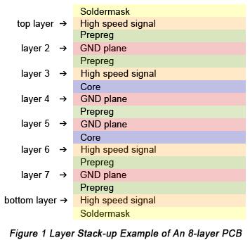
A stack-up refers to the arrangement of the copper and insulating layers that make up a PCB before starting board layout design. For multilayer PCBs, general layers include ground layer, power plane, signal layer, high speed signal layer, solder mask and silk screen. Figure 1 shows an 8-layer PCB stack-up example.

From this figure, it's obviously clear to indicate that layer distribution in a PCB follows a symmetrical or balanced structure. Besides the eight layers, the spacing between layers should be taken seriously as well. In order to meet the requirement of miniaturization, while planning a layer stack-up, minimum trace spacing must be obtained. The space between layers can be either core or prepreg. Generally speaking, multilayer boards consist of at least one or more cores and prepreg. Cores are made up of a copper-plated glass-reinforced epoxy laminate sheets. The thickness of core is in the range from 0.1mm to 0.3mm.
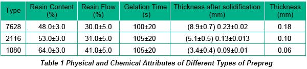
Prepreg is the common term for a reinforcing fabric which has been pre-impregnated with a resin system. This resin system (typically epoxy) already includes the proper curing agent. The main function of prepreg is its role in stacking all layers into a whole board by high temperature stack-up. Prepreg has the following main categories: 7628, 2116 and 1080 whose physical and chemical attributes are displayed in Table 1.
Actually, thickness of each type of prepreg isn't usually stable and some adjustments will possibly be made in order to meet the specific board thickness requirement. Some factors have to be taken into consideration when determining the number of prepreg including thickness of inner layer, product design thickness requirement or technique requirement, prepreg type, practical performance and the actual thickness after stack-up trial. For example, Figure 2 shows a 4-layer PCB thickness example.
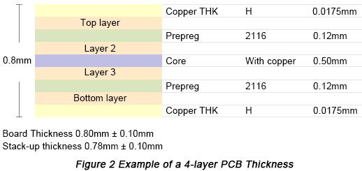
In this example, the thickness of copper thickness is stable so that the thickness of prepreg and core should be adjusted in order to meet the whole thickness requirement.
Some solutions to possible problems in the process of stack-up
• Interlayer offset
Resin recession groove is used in board side design instead of choked flow pad. In regards with stack-up positioning, hot melting plus rivet plus dowel method can be used to solve stack-up offset problem.
• Stack-up measling
In the process of board arrangement, silicon pads can be added, together with the assistance of epoxy plate so that pressure will remain balanced, which can both help eliminating stack-up measles and effectively control the uniformity of board thickness.
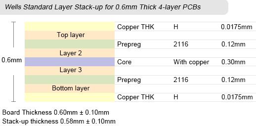
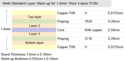
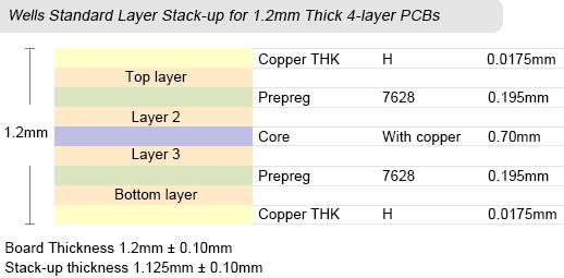
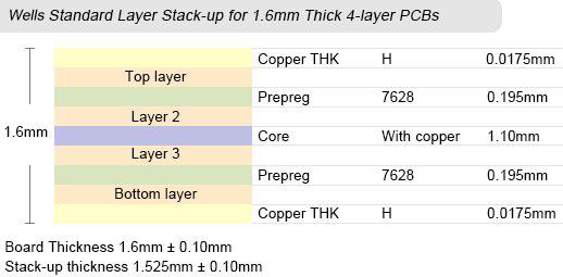
Wells Standard PCB Layer Stack-up
As for standard multilayer boards, PCB can provide boards with layers in the range from 4 to 32 layers, board thickness from 0.4mm to 3.2mm, copper thickness from 18µm to 210µm (0.5oz to 6oz), inner layer copper thickness from 18µm to 70µm (0.5oz to 2oz), and minimal spacing between layers to 3mil.
Images below display PCB's standard stack-up capabilities and dimensions. Did not find the layer stack-up for your custom circuit boards? Simply inform us your PCB thickness and layer numbers at sales@wellspcba.com, we'll provide the corresponding stack-up very quickly.
Note: we use default layer stack-up for PCB Prototype Service. If you do not accept our default layer stack-up, please switch to our Standard PCB Service.

Welcome to get the customized multilayer pcb with our professional manufacturers and suppliers. Through strict manufacturing process, we can assure you of the high quality and high efficiency of our multilayer pcb. Please be free to contact our factory.
-
HDI PCB 1 Pieces / (Min. Order)
-
PCB Board Assembly Service Double-sided 5 Pieces / (Min. Order)
-
PCBA Assembly For Smart Home Camera 5 Pieces / (Min. Order)
-
Final Product Function Test 1 Pieces / (Min. Order)
-
PCBA Board Function Test 1 Pieces / (Min. Order)
-
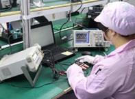
On Board Programming 1 Pieces / (Min. Order)
-
Wire Harness Assembly 1 Pieces / (Min. Order)
-
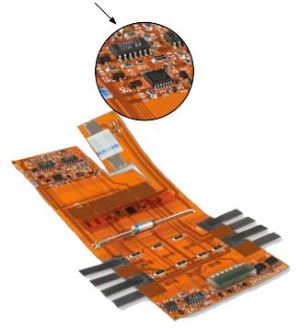
Flexible PCB Assembly 1 Pieces / (Min. Order)
-
Dip Through Hole PCBA 1 Pieces / (Min. Order)
-
SMT PCBA 1 Pieces / (Min. Order)
-
PCB Assembly Service 1 Pieces / (Min. Order)
-
HDI PCB 1 Pieces / (Min. Order)
 Favorites

-
PCB Board Assembly Service Double-sided
5 Pieces / (Min. Order)
-
PCBA Assembly For Smart Home Camera
5 Pieces / (Min. Order)
-
Final Product Function Test
1 Pieces / (Min. Order)
-
PCBA Board Function Test
1 Pieces / (Min. Order)
-
On Board Programming
1 Pieces / (Min. Order)
-
Wire Harness Assembly
1 Pieces / (Min. Order)
-
Flexible PCB Assembly
1 Pieces / (Min. Order)
-
Dip Through Hole PCBA
1 Pieces / (Min. Order)
-
SMT PCBA
1 Pieces / (Min. Order)
-
PCB Assembly Service
1 Pieces / (Min. Order)
-
HDI PCB
1 Pieces / (Min. Order)