

PCB Board Assembly Service Double-sided
-
Payment


-
Origin
China Mainland
-
Minimum Order
5
-
Packing
Pieces
- Contact Now Start Order
- Description
Product Detail
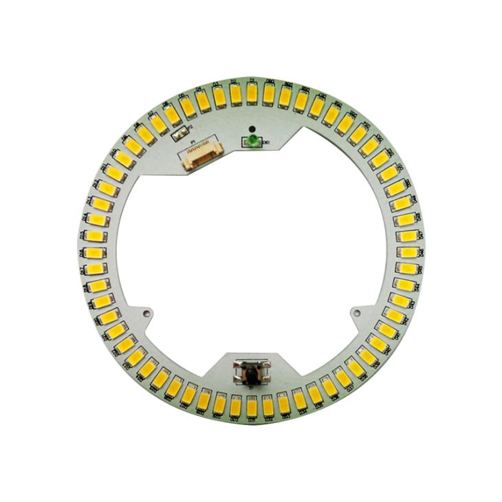
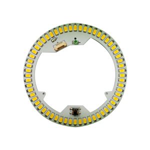
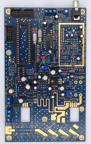
PCB Assembly Sample Introduction
Product Details:
Place of Origin: | China |
Brand Name: | OEM |
Certification: | CE,ROHS, FCC,ISO9008,SGS,UL |
Model Number: | OEM |
Payment & Shipping Terms:
Minimum Order Quantity: | 1pcs |
Price: | negotiation |
Packaging Details: | inner: vacuum-packed bubble bag? outer: carton box |
Delivery Time: | 5-10 days |
Payment Terms: | T/T,Western union |
Supply Ability: | 1, 000, 000 PCS / week |
Detailed Product Description
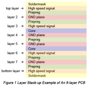
Material: | FR4 | Layer: | 2 |
Color: | Green | Min Line Space: | 10mil |
Min Line Width: | 10mil | Copper Thickness: | 1OZ |
Size: | 5*4cm | Board THK: | 1.0MM |
Panel: | 4*5 | Surface Finish: | HASL |
Model: | XCEA | Brand: | XCE |
High Quality Electronics Products PCB / PCBA Assembly Service
NO | Item | Craft Capacity |
1 | Layer | 1-30 Layers |
2 | Base Material for PCB | FR4, CEM-1, TACONIC, Aluminium, High Tg Material, High Frequence ROGERS ,TEFLON, ARLON, Halogen-free Material |
3 | Rang of finish baords Thickness | 0.21-7.0mm |
4 | Max size of finish board | 900MM*900MM |
5 | Minimum Linewidth | 3mil (0.075mm) |
6 | Minimum Line space | 3mil (0.075mm) |
7 | Min space between pad to pad | 3mil (0.075mm) |
8 | Minimum hole diameter | 0.10 mm |
9 | Min bonding pad diameter | 10mil |
10 | Max proportion of drilling hole and board thickness | 1:12.5 |
11 | Minimum linewidth of Idents | 4mil |
12 | Min Height of Idents | 25mil |
13 | Finishing Treatment | HASL (Tin-Lead Free), ENIG(Immersion Gold), Immersion Silver , Gold Plating (Flash Gold), OSP, etc. |
14 | Soldermask | Green, White, Red, Yellow, Black, Blue, transparent photosensitive soldermask, Strippable soldermask. |
15 | Minimun thickness of soldermask | 10um |
16 | Color of silk-screen | White, Black, Yellow ect. |
17 | E-Testing | 100% E-Testing (High Voltage Testing); Flying Probe Testing |
18 | Other test | ImpedanceTesting,Resistance Testing, Microsection etc., |
19 | Date file format | GERBER FILE and DRILLING FILE, PROTEL SERIES, PADS2000 SERIES, Powerpcb SERIES, ODB++ |
20 | Special technological requirement | Blind & Buried Vias and High Thickness copper |
21 | Thickness of Copper | 0.5-14oz (18-490um) |
Product type:
Single-sided, double-sided and multilayer printed circuit boards (PCB), flexible (soft) of circuit boards, blind buried plate.
Max size: single-sided, double-sided: 1000mm * 600mm MLB: 600mm * 600mm
Highest Number of floors: 20 floors
Processing board thickness: 0.4mm -4.0mm rigid plate flexible plate 0.025mm --- 0.15mm
Copper foil substrate thickness: rigid plate 18µ (1 / 2OZ), 35µ (1OZ), 70µ (2OZ) flexible board 0.009MM 0.018mm 0.035mm 0.070mm 0.010mm
Common substrates: FR-4, CEM-3, CEM-1, 94HB, 94VO, poly vinyl chloride, polyester, polyimide ammonium.
Process Capability:
(1) Drilling: Minimum aperture 0.15MM
(2) metal hole: Minimum aperture 0.15mm, thickness / aperture ratio of 4: 1
(3) wire width: Minimum width: gold plate 0.075mm, 0.10mm tin plate
(4) lead spacing: Minimum spacing: gold plate 0.075mm, 0.10mm tin plate
(5) gold plate: Ni layer thickness:> or = 2.5µ gold layer thickness: 0.05-0.1µm or according to customer requirements
(6) HASL: tin layer thickness:> or = 2.5-5µ
(7) paneling: Wire-to-edge minimum distance: 0.15mm hole to edge minimum distance: 0.2mm Minimum Shape tolerance: ± 0.12mm
(8) outlet chamfer: angle: 30 degrees, 45 degrees, 60 degrees Depth: 1 -3mm
(9) V cut: angle: 30 degrees, 35 degrees, 45 degrees Depth: 2/3 thickness minimum size: 80mm * 80mm
(10) off test:
Resistance to soldering heat: 85 --- 105 ? / 280 ? --- 360 ?
Flexible sheet resistance flexing resistance / chemical resistance: full compliance with international standards
Inspection:
1. The main inspection hole metallization quality status, should ensure that the hole was no extra burr, black holes, holes and so on;
2. Check the substrate surface dirt and other unwanted objects;
3. Check the board number, drawing number, process documentation and process description;
4. clarify racking parts, racking requirements and can withstand the plating tank plating area;
5. plating area, the process parameters to be clear, to ensure the stability and viability of the electroplating process parameters;
6. conductive parts cleaning and preparation, the solution was presented first energization process active;
7. finds bath composition is checked, plate surface area status; such as the use of spherical anode bar installed, you must also check the consumption;
8. Check the voltage solid case and the contact area, the current fluctuation range.
-
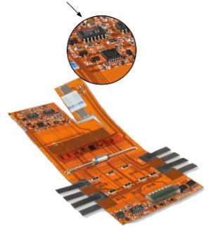
PCBA Assembly For Smart Home Camera 5 Pieces / (Min. Order)
-
Wire Harness Assembly 1 Pieces / (Min. Order)
-
Flexible PCB Assembly 1 Pieces / (Min. Order)
-
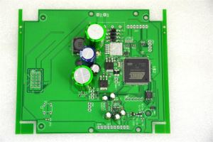
Dip Through Hole PCBA 1 Pieces / (Min. Order)
-
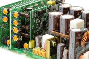
SMT PCBA 1 Pieces / (Min. Order)
-
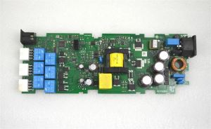
PCB Assembly Service 1 Pieces / (Min. Order)
 Favorites

-
PCBA Assembly For Smart Home Camera
5 Pieces / (Min. Order)
-
 Final Product Function Test
1 Pieces / (Min. Order)
Final Product Function Test
1 Pieces / (Min. Order)
-
 PCBA Board Function Test
1 Pieces / (Min. Order)
PCBA Board Function Test
1 Pieces / (Min. Order)
-
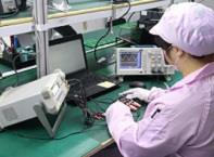
 On Board Programming
1 Pieces / (Min. Order)
On Board Programming
1 Pieces / (Min. Order)
-
Wire Harness Assembly
1 Pieces / (Min. Order)
-
Flexible PCB Assembly
1 Pieces / (Min. Order)
-
Dip Through Hole PCBA
1 Pieces / (Min. Order)
-
SMT PCBA
1 Pieces / (Min. Order)
-
PCB Assembly Service
1 Pieces / (Min. Order)
-
 Multilayer PCB
1 Pieces / (Min. Order)
Multilayer PCB
1 Pieces / (Min. Order)
-
 HDI PCB
1 Pieces / (Min. Order)
HDI PCB
1 Pieces / (Min. Order)